歡迎光臨~泰州巨納新能源有限公司
語言選擇:
 ∷
∷

∷
 ∷
∷


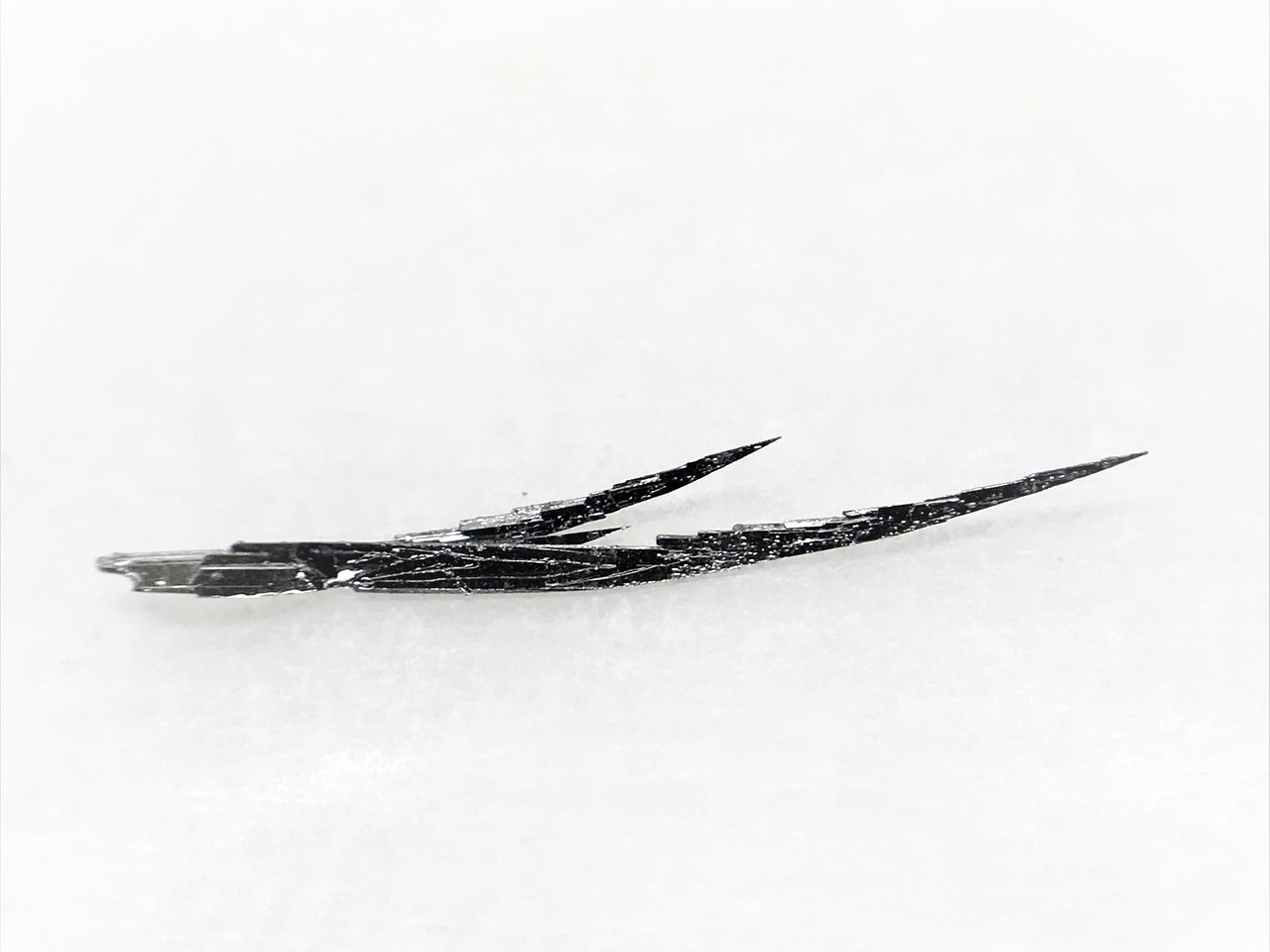
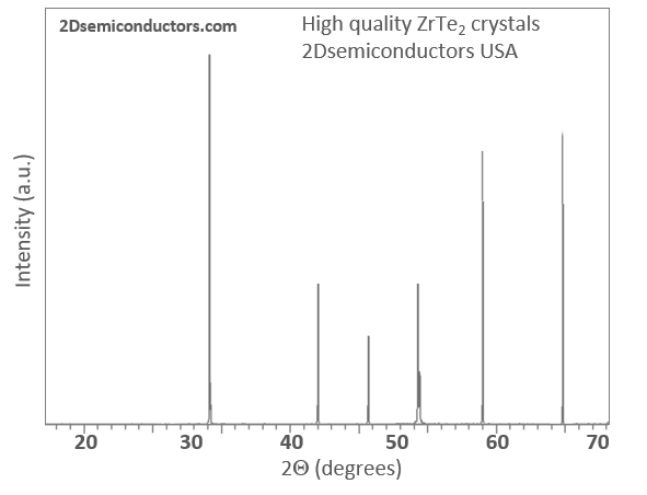
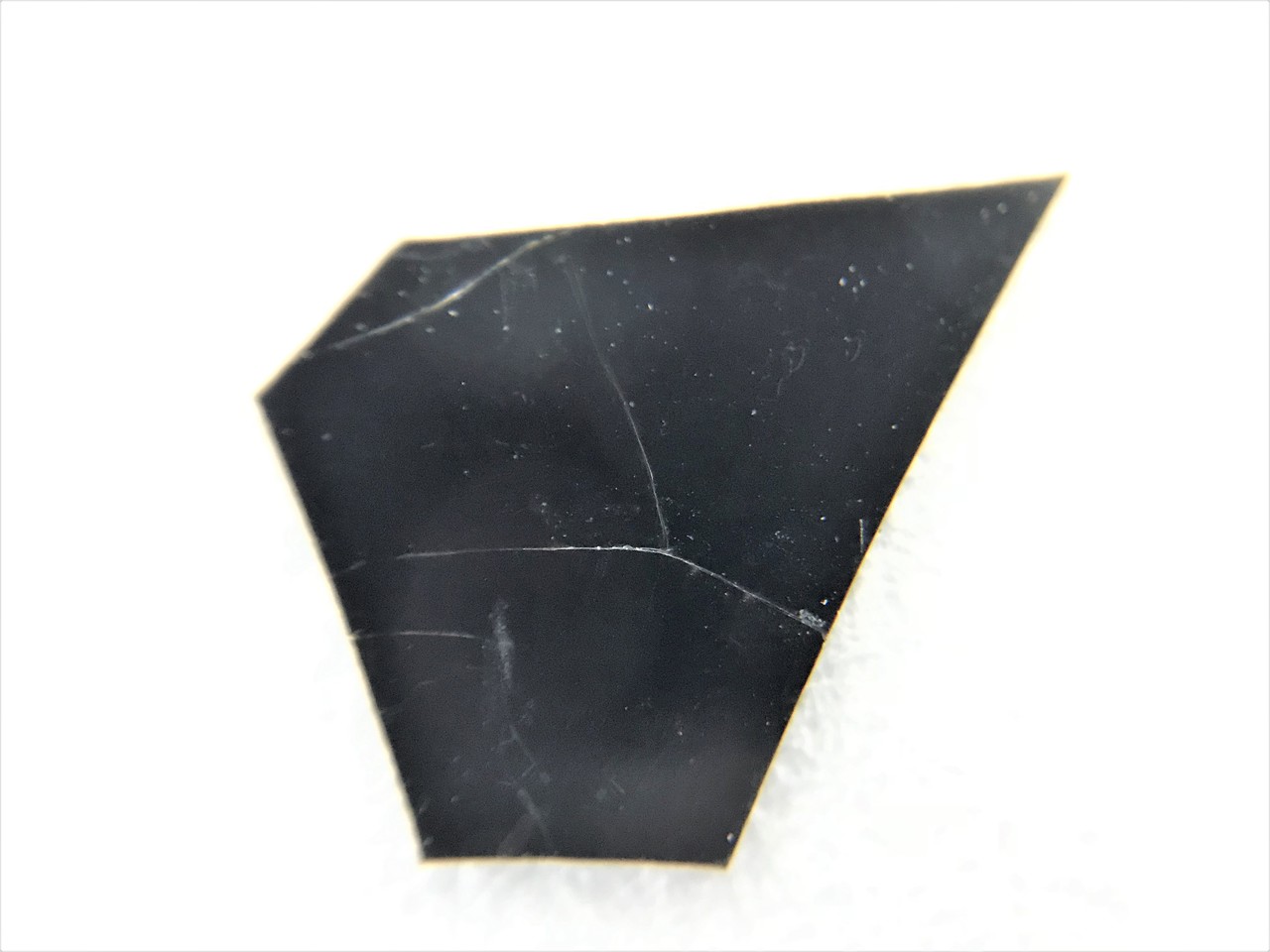
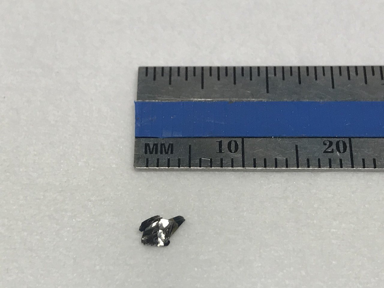
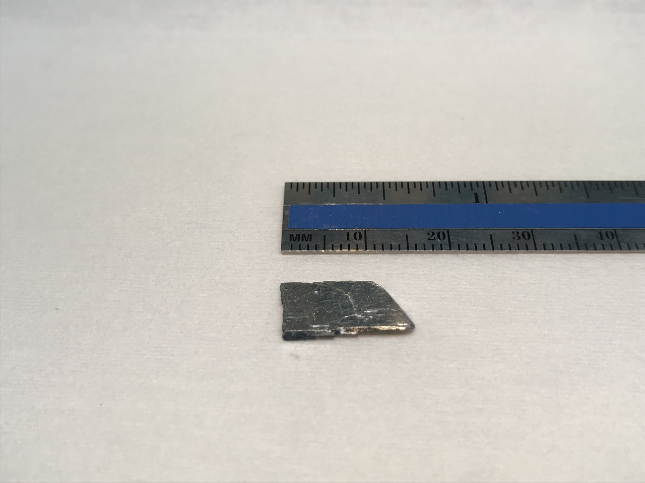
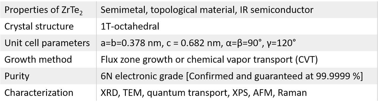
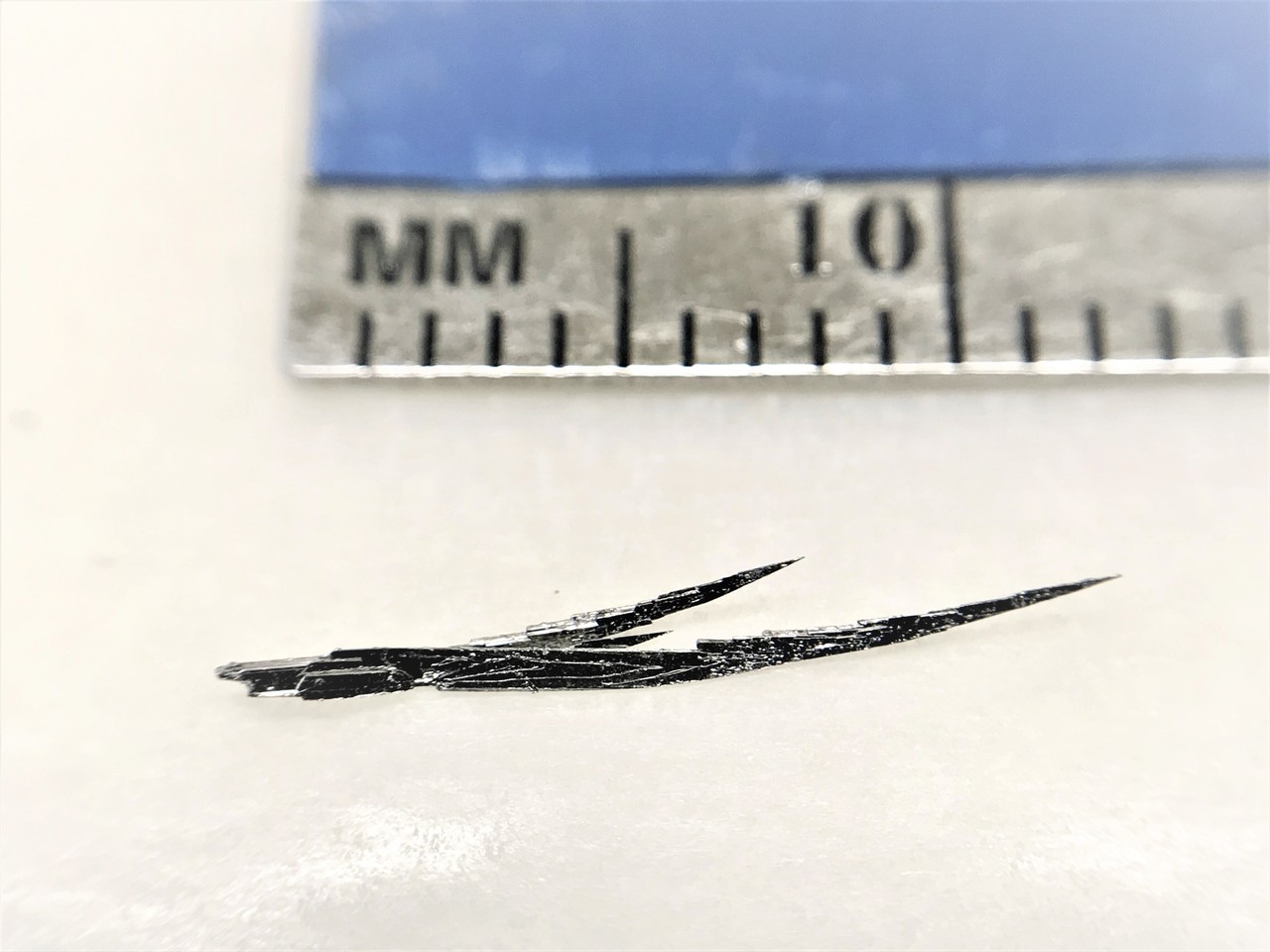
ZrTe2 belongs to group-IV TMDCs family and adopts a stable 1T-octahedral structure. ZrTe2's eelectronic bandstructure has interesting characteristics showing crossings of valence and conduction bands, near the Fermi level suggesting topological 3D Dirac semimetal behavior [1]. Interestingly, DFT calculations have also shown opening of electronic band gap for sheets below 3-4 layers, and becomes direct gap semiconductor in monolayer form (Egap~0.3-0.5 eV). These ZrTe2 crystals were designed and optimized at our facilities starting 2014 to achieve perfect electronic grade materials with: 1) excellent stoichiometry, 2) large single domain size, 3) single phase materials without any mixed phases or amorphous content, 4) unmatched purity -electronic grade (5.8N), 99.9998% confirmed. Our crystals exhibit sharpest Raman and XRD peaks in the commercial market proving the high quality of our materials.purity.
Properties of ZrTe2 layered crystals
Growth method matters> Flux zone or CVT growth method? Contamination of halides and point defects in layered crystals are well known cause for their reduced electronic mobility, reduced anisotropic response, poor e-h recombination, low-PL emission, and lower optical absorption. Flux zone technique is a halide free technique used for synthesizing truly semiconductor grade vdW crystals. This method distinguishes itself from chemical vapor transport (CVT) technique in the following regard: CVT is a quick (~2 weeks) growth method but exhibits poor crystalline quality and the defect concentration reaches to 1E11 to 1E12 cm-2 range. In contrast, flux method takes long (~3 months) growth time, but ensures slow crystallization for perfect atomic structuring, and impurity free crystal growth with defect concentration as low as 1E9 - 1E10 cm-2. During check out just state which type of growth process is preferred. Unless otherwise stated, 2Dsemiconductors ships Flux zone crystals as a default choice.


聯系人:嚴春偉
手機:13914543285
電話:0523-86190619,86192878
郵箱:taizhou@sunano.com.cn
地址: 江蘇省泰州市鳳凰西路168號