歡迎光臨~泰州巨納新能源有限公司
語言選擇:
 ∷
∷

∷
 ∷
∷
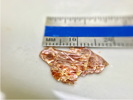
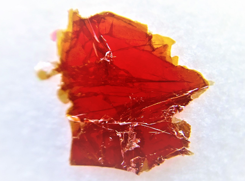
Our newest class of material: Sb2xAs2(1-x)S3 comes in perfect 1:1:3 stoichiometry consisting of Sb-Sb-S3 atoms. After 34 growth trials in a year, perfect stoichirometry, large single crystal domain size, minimal defect density (1 parts in 100,000 unit cells), and perfected purity level (99.9998%) are achieved. In the bulk form, antimony arsenic sulfide (SbAsS?) is a direct gap semiconductor and has band-gap at around 1.7 eV. Similar to molybdenum disulfide, it has layered structure (lamellar) with weak interlayer coupling and can be isolated down to monolayers. The monolayer thickness measures ~0.8 nm and the monolayer SbAsS? is waiting to be discovered both experimentally and theoretically. Our crystals are large in size ~5-8mm and show remarkable PL characteristics.
Our crystals are grown by state-of-the-art growth techniques over 8 weeks and show high crystallinity. Raman spectrum displays very sharp and clear modes with FWHM less than 6cm-1. Single crystal SbAsS? comes ready for exfoliation and is ideal for 2D research.
Summary:
Sb2xAs2(1-x)S3 alloys are created by alloying Sb into As2S3.
Please specify your x value when ordering
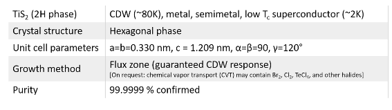
Space group: P21/c
Layered: Yes / Exfoliates to monolayers
Band gap: ~1.7 eV in bulk
Purity: Semiconductor grade (6N) 99.9999%
Growth technique: Vapor transport technique – Duration: 2.0 months
Sample size: 5-10 mm
聯系人:嚴春偉
手機:13914543285
電話:0523-86190619,86192878
郵箱:taizhou@sunano.com.cn
地址: 江蘇省泰州市鳳凰西路168號